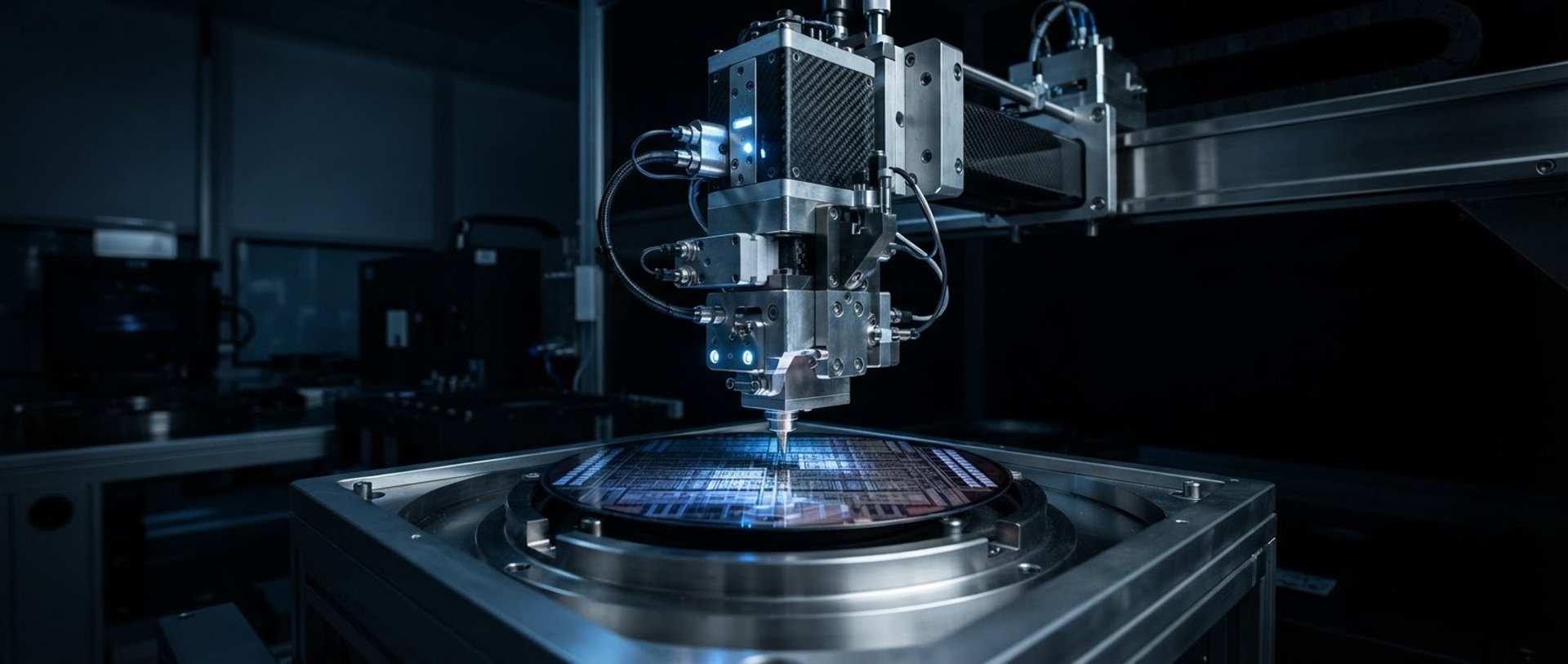
Sub-nanometer tool physics
We resolve critical yield bottlenecks, micro-vibrations, and thermal drift anomalies across high-vacuum lithography and deposition systems.
Verified tool expertise
First-principles physical solutions engineered directly for Tier-1 lithography, deposition, and etch hardware platforms globally.
EUV & DUV Optics
ALD & CVD Chambers
Plasma Systems
Mitigating sub-angstrom thermal drift and wavefront errors in projection lens assemblies and ultra-high-speed wafer stages.
Optimizing gas-flow boundary layers and thermal uniformity to eliminate sub-nanometer thickness variations across the wafer.
Stabilizing high-density RF plasma fields and electrostatic chuck temperatures to prevent critical feature size drift.
First-principles verification
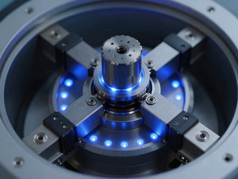
We do not rely on empirical trial-and-error. Our former OEM principal designers construct multi-physics thermal and mechanical models to isolate the precise root cause of sub-angstrom yield loss.
Every physical modification is simulated under full cleanroom vacuum and thermal load conditions before hardware fabrication begins, ensuring drop-in compatibility with existing toolsets.
Resolve tool bottlenecks
Engage our elite engineering team under strict NDA to diagnose and eliminate thermal drift, micro-vibrations, or yield losses.
Aryllium Technology
Transform Quality Problems Into Engineering Solutions
CENTERS OF EXCELLENCE
Singapore - Texas - California
eMail: solutions@aryllium.com
© 2026 Aryllium Technology
SUB-ANGSTROM PRECISION